


Why SMD PCB stencil?
SMD elements expanding a greater thickness and parts on the motherboard. The PCB stencil soldering procedure does not influence making use of a soldering wave, even in a reflow oven or making use of vapor phase soldering. The possible tin solder is loosened up in the form of a paste using a stencil and also squeegee. The parts are after that noted on the solder paste. The sticky pressure of the paste avoids it from diminishing. Larger parts are typically Glued to it.
-
Why SMD PCB stencil?
SMD elements expanding a greater thickness and parts on the motherboard. The PCB stencil soldering procedure does not influence making use of a soldering wave, even in a reflow oven or making use of vapor phase soldering. The possible tin solder is loosened up in the form of a paste using a stencil and also squeegee. The parts are after that noted on the solder paste. The sticky pressure of the paste avoids it from diminishing. Larger parts are typically Glued to it.
SMD Assembly MOKO Printed Circuit Board Assembly Offers thorough solutions for putting together surface-mounted (SMD) parts and also parts for push-through setting up (THT). Our production center is technologically flexible, we tackle the setting up of numerous components from the SMD elements of dimension 0201 to the integrated circuits with QFP and also BGA & uBGA real estates in outstanding top quality with a lot of experience. Our regular collection dimension is in between 1 and also 1000 items, the regular order duration is 5 to 10 days.
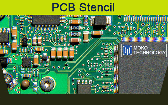
SMD assembly PCB stencil
Develop solder paste PCB stencil 9 Action:
Step 1: Product and also prep work
Step 2: Prepare the PCB format and also identify dimensions
Step 3: Produce Gerber data
Step 4: Open Gerber file for conversion
Tip 5: Export Gerber to SVG file
Action 6: Cutting software program
Action 7: Modification The dimension of the style
Tip 8: Prepare openness and also equipment
Step 9: Cut your pattern
Utilize a Cricut cutting maker and also Sure-Cuts-A-Lot software program to develop usable solder paste stencils for digital prototyping purposes.
The high quality as well as precision of the patterns acquired are good enough, size 0805 and also TQFP (0.8 mm pitch) digital component prototype.
This Instructable on a tutorial I originally wrote based upon solder paste stencils.
I would certainly not recommend buying a Cricut simply to create solder paste stencils. Nevertheless, if you have a friend or relative that owns one, or at a Cricut shop or at the flea market, then acquiring Sure-Cuts-A-Lot software will certainly transform a Cricut right into an extremely valuable gadget. Performance after that comes to be something like a low-end vinyl/craft cutter like its Craft Robo.
Action 1: Product and also prep work for PCB stencil Products
-- Cricut device -- Sure-Cuts-A-Lot software -- Gerber audience software application -- Transparencies for overhead projectors that you can purchase any workplace supply store -- A Windows XP/ View computer
Prep work
Your Cricut needs to have a particular firmware variation. You can update/downgrade the firmware by downloading and install Cricut Layout Workshop and complying with the guidelines under Aid to update the firmware. See the Sure-Cuts-A-Lot FAQ to find out more.
Step 2: Prepare the PCB format and also establish dimensions It can take some trial and error to develop respectable solder paste PCB patterns is not very precise. It reduces rounded sides as well as disregards shapes smaller than concerning 18mil (0.46 mm) by 50mil (1.27 mm). That said, you ought to make sure that every one of your element pads are big than these. To ensure a pad still has adequate solder paste area, make the pad a lot more. The KiCAD EDA Collection PCB layout program has the ability to alter all one impact pads at a time. Solder has this remarkable home that links to metal parts when reflow discovers. As long as your PCB has accurate solder stand up to, solder metal pieces will be found to web link. So do not be also worried regarding pads (primarily claim +/- 20%).
You require the specific measurements of your PCB template for later. Use your PCB design software distance device to determine the distance between the outermost element pads. Not the size of the PCB, but the range between outer pad edges. In the example listed below, the PCB has a size of 2.3 ", but the edge to border pad distance is 2.142".
You can determine ranges by selecting illustrations from the layer pull-down menu as well as clicking the Capacities button in the right tool food selection. It's the 4th button from the bottom.
Step 3: Producing Gerber documents Attract your PCB format making use of the Gerber solder paste stencil.
When utilizing KiCAD, select Draw from the Data menu. In the plot home window, pick SoldP_Cmp for the solder paste component layer as well as click the Story button.
Step 4: Open Gerber apply for conversion Open up the documents in Gerber Customer. Select Open Layer (s) from the Data menu.
Tip 5: Export Gerber to SVG file After that export the documents in SVG layout. Select Export, after that SVG ... from the File food selection.
Action 6: Cutting software Produce solder paste patterns with Cricut Import the SVG data right into Sure-Cuts-A-Lot by selecting Import SVG ... from the Data menu.


Join the Discussion