


Regular Mistake Categories for BGA PCB Soldering Joints
The underside of the chip articulated. BGA PCB innovation has many contrasted to wired IC advantages such as: - Smaller sized housing - Greater packaging thickness - Greater pin density - Enhanced signal transmission homes - Better thermal coupling to the circuit card
-
-
The underside of the chip articulated. BGA PCB innovation has many contrasted to wired IC advantages such as: - Smaller sized housing - Greater packaging thickness - Greater pin density - Enhanced signal transmission homes - Better thermal coupling to the circuit card
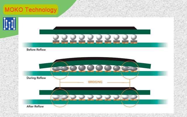
Newest types of these parts, such as which make it possible for VFBGA (Extremely Great BGA) on the other hand a number of thousand link pins with a pitch of less than 0.5 mm. The BGA PCB components are set up in a corresponding soldering procedure, with lots of elements play a role. The outcome of this procedure is normally a matt.
- High degree of liability in between the round and also motherboard
- High mechanical long-lasting security
- The high architectural stability of the sphere body
- High conductivity
- High electrical signal honesty
- High insulation resistance to surrounding pins
At this point the interaction in between the physical states and the resulting electrical buildings plainly. The recommendation version shows the structural relationships in a streamlined fashion. It is based on a static, directional signal with easy ohmic. The problems dominating in the chip (bond cords, etc) are neglected too understood.
Fixed recommendation version in between the mechanical as well as the electric level during the soldering process, the solder of the spheres thaws with the solder paste as well as it forms a chemical reaction with the surface of the motherboard an intermetallic area. Additionally, there is an intermetallic area between the chip and also the ball body, which, nonetheless, is pronounced at the chip maker and must also be inspected by him. This need to generally be in between the transmitter and also the receiver need to be steady at the milliohm level.
But all theory is grey since in practice both organized and also random occur errors and these lead to significantly transformed electrical specifications and additionally one glossy solder joint is by no means a guarantee of freedom from mistakes. They range from visible deformations of the solder body in the senses of lean or fat solder joints, where there is electrical call, as much as optically distinct solder joints without, or sporadically dropping electric call.
The conventional IPC-A-610E plays a vital duty in the assessment of a BGA PCB soldering joint duty. It defines the acceptance standards for electronic settings up and additionally specifies criteria for MOKO Printed Circuit Board Assembly. So for a production system remedies are necessary which make sure the conformity of the solder joints to this standard can show. This additionally causes structurally unpredictable solder joints where it is underneath mechanical stress to damage and also therefore to loss of electrical conductivity comes avoided. However, it continues to be to be kept in mind that several errors, the shape of the solder body regarding, just have electrical impacts at severe values.
Worth discussing right here are the "Head in Cushion" as well as "Black Pad "well-known sensations. With the previous impact, the solder does not thaw with the solder paste and also a quasi-barrier layer is created. Nevertheless, the optics of the solder joint expose this generally not. The major causes, in this case, are contamination of the sphere surface area.
The trouble with the black pad is much more in the direction of the circuit board. Below the responds sphere with the solder paste yet below it additionally creates a layer with decreased or complete lack of conductivity.
Review of typical error classifications for BGA PCB soldering joints SeverityMechanical/ Optical appearanceselectrical appearancespotential causes Faulty Lotkorpusincorrect round form -- inaccurate surface -- pores (spaces). -- Incorrect placement. -- Incorrect solder round distance. -- absence of co-planarity-- RBK barely changed. -- RBK = ∞ (open link). -- Short circuit in between rounds-- BGA-Chip (Round)-- Lotpastenqualität-- Lotpastenauftrag-- Montageversatz-- Lötprofil-- Pad-Design. responsibility weakness. between sphere and. solder paste. " Head in Pillow"-- correct round form. -- contamination layer. between round and also solder paste. -- No mechanical. load-bearing capacityRIZ = ∞ (open connection). -- Short-term call with. mechanical loadBGA-Chip (Round). -- Lotpastenqualität. -- Lötprofil. obligation weak point. between solder joint. as well as circuit board. " Black Pad"-- appropriate spherical form. -- contamination layer. between sphere as well as solder paste. -- cracks in the intermetallic area. -- Dark pad discoloration. -- low mechanical. Resilience (demolition)-- RIZ = ∞ (open link). -- leads to mechanical tension. for momentary call. -- RIZ in the normal variety,. Connection breaks off. Load (open solder joint)-- PCB high quality.


Join the Discussion