


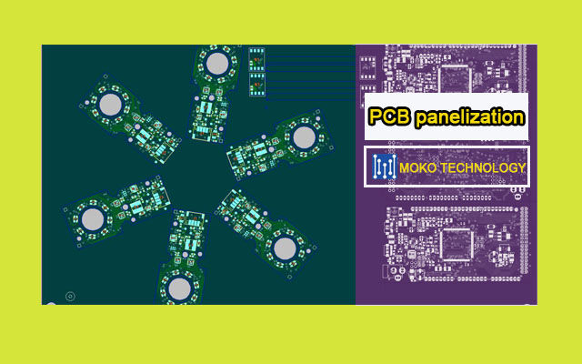
Different PCB Panelization Approaches
Different approaches of PCB panelization Similar to many procedures in the electronic devices industry, there are numerous opportunities and also variations in the PCB panelization. Considering that each maker has its own technique, you as a designer have to select from time to time to adjust your design accordingly or to search for a different companion for manufacturing. The 3 most common methods are clarified listed below:
-
Different PCB Panelization Approaches
Different approaches of PCB panelization Similar to many procedures in the electronic devices industry, there are numerous opportunities and also variations in the PCB panelization. Considering that each maker has its own technique, you as a designer have to select from time to time to adjust your design accordingly or to search for a different companion for manufacturing. The 3 most common methods are clarified listed below:
Panelization making use of V-grooves: With this strategy, the private circuit card are divided from each other by V-shaped milled grooves with a depth of one-third of the panel elevation. The later splitting up is after that carried out by a device that is finest fit for straight cuts. This approach is as a result specifically suggested for PCBs that meet 3 demands: no overhanging parts, no rounded corners and also an adequate range in between the part restriction and the side of the PCB.
Panelization with tab transmitting: Here, the motherboard are crushed out along their shapes-- while keeping a handful of product bridges that hold the board safely in place throughout the manufacture and setting up of the panel. This kind of panelization is not appropriate for printed motherboard with large transformers and other larger elements that considerably complicate the splitting up. At the same time, it needs to be noted that this method reduces the tons on the printed circuit boards as well as thus decreases the risk of breaking.
Panelization through tab directing with perforated product bridges: This process resembles the easy tab directing simply defined. However, right here the product bridges are in addition perforated with small drill holes, which considerably simplifies the separation and additionally supplies a higher degree of control since the training course of the fracture is less complicated to forecast. However, this method is even much less suitable for printed circuit boards with hefty elements, the weight of which can damage the material bridges.
PCB panelization
The downsides of PCB panelization Paneling PCBs is one method to secure its honesty. On top of that, panelization enables China PCB suppliers to put together numerous boards at the same time, minimizing expenses and also production time. The paneling should be performed effectively to ensure that the printed circuit card are not harmed or otherwise damaged during the separation.
Obstacles: Paneling provides a number of obstacles in numerous locations: 1. Depanelization- downsides of some depanelization methods: If using a router, added cleansing might be required prior to shipping. This approach creates a lot of dust that has to be drawn out.
Substitute of components pre-routing called for to avoid disturbance with depanelization: Extending components can come under adjacent components.
Incomplete information documents-- sometimes incomplete data are given by MOKO PCB Assembly, which can increase costs in numerous means: " Breakaway holes" or "computer mouse attacks"-- These little holes allow the use of little motherboard in a variety.
Cumulative and Enrollment Tolerances-- If there are no limited resistances in the information documents, the cumulative impact of tiny variances can lead to mistakes. If there are several boards in the array, the registration can no longer be focused.
DFM and PCB panelization When firms develop published motherboard for huge quantities, they search for means to lower production prices with little methods and techniques. This needs just reasonably little initiative if the information of the production are reviewed thoroughly in the early stage of the style procedure and thought about in the advancement of the printed circuit card (which is consequently highly advised). This very early optimization of the format with regard to the prepared manufacturing processes is typically referred to as "production-oriented design" or "Style for Production" (short: DFM).


Join the Discussion